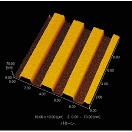
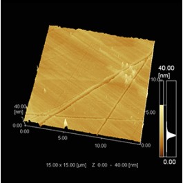
Wafer Structure (1)
Scanning results of wafer structure on a nanometer scale
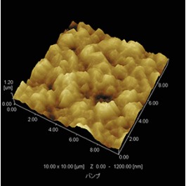
Wafer Structure (2)
Scanning results of structural bumps on wafer
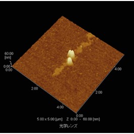
Optical Lens Examination
Detection of foreign body on optical lens
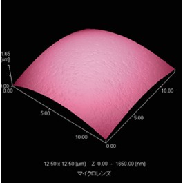
Micro-lens Structure
Scanning results of micro-lens surface structure
Stainless Plate Structure
Scanning results of topographic structure on stainless plate
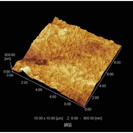
Copper Foil Structure
Scanning results of surface structure on copper foil
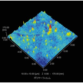
Polymer Film Structure
Scanning results of topographic structure on polymer film
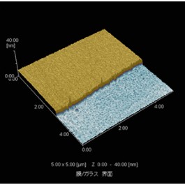
Thin Film Boundary
Scanning examination of topographic structure on thin film boundary